
Recently, I have been developing a watch (miniature) version of ClockSquared. One of the main challenges for this device is to achieve good battery life while not making the watch excessively large or hard to use. This can be achieved by taking various power-saving measures that I will discuss in a future post, but what I will discuss today is way to actually verify that the watch’s power consumption is sufficiently low while in use and while in “sleep mode”.
Dave Jones, the author of EEVBlog, developed a great little device that enables the user to measure electrical currents (in ampere), all the way from the pico scale to the base scale. The main advantage of this device is that it does this with very low burden voltage, a concept which is nicely explained by Dave Jones himself here, or by Andreas Spiess here.
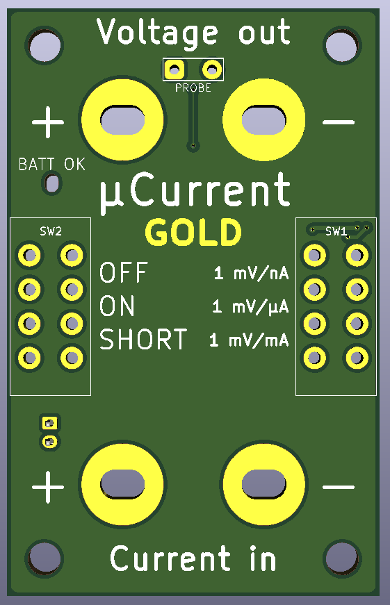
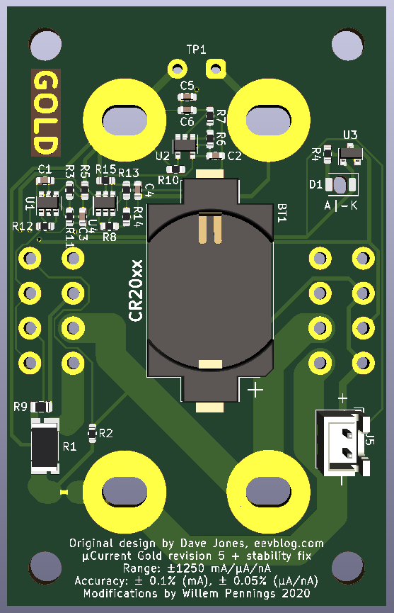
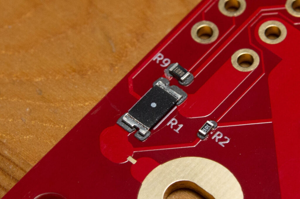
The uCurrent Gold is open source hardware and I took advantage of this by porting the PCB documents to KiCad and adding several improvements. Firstly, I added two 0.1 uF decoupling capacitors between the V+ and V- rails and ground (C5, C6) to improve the robustness of the measurement system. Secondly, I added a footprint for a JST-XH connector (J5) which allows the device to be powered by an external battery, e.g. 3xAA batteries. (The higher voltage will also increase the ranges!) Lastly, I added a probe connection point (TP1), which I hope will allow lower-noise measurements (if I ever purchase a scope, that is). I also simplified the silkscreen a bit. Here is a front and back view of the PCB in KiCad’s 3D viewer (some components not shown):
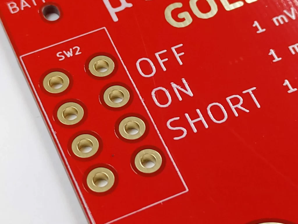
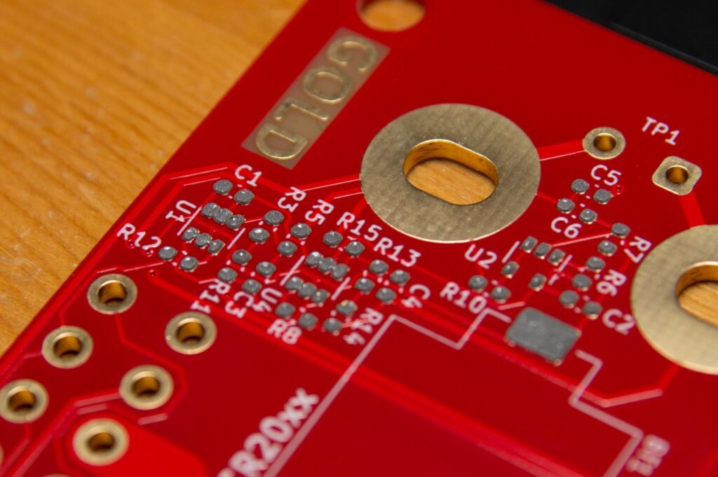
The PCBs were manufactured by PCBWay. PCBWay was very kind to support my work and supply these PCBs to me free of charge in return for an evaluation of the quality of the PCBs. I chose an ENIG finish, red silkscreen and 1.6 mm thick PCB, like the original uCurrent. Below are some close-up photos of the unassembled PCBs.


Assembling it
This project will be my first reflow soldering project. Reflow soldering is a soldering process that allows many components to be soldered to a PCB in one go. Contrary to using solder wire and a soldering iron, this process works by dispensing solder paste onto a PCB, placing components on the PCB and subsequently reflowing the PCB in an oven to create the mechanical and electrical connection between the PCB pads and component leads. I’ve been assembling ClockSquared Mini prototypes using hand soldering techniques and to be fair, it is quite annoying and difficult to get right. Reflow soldering makes the assembly process easier, quicker and less prone to errors.

The first step in the process is to align the SMT stencil with the PCB’s solder pads. Many prototype PCB manufacturers offer stencil manufacturing services too, so these can be ordered together with the PCBs. Once the stencil is positioned correctly, I secure it in place using tape. I noticed how the stencil contains a lot of scratching. Perhaps the factory used some sort of abrasive tool to deburr the apertures? I’m not sure if burrs are formed in the cutting process.
Solder paste is subsequently applied to the stencil. Using a squeegee, the solder paste is distributed over the stencil and finds its way into the apertures. When all apertures are filled with solder paste, the stencil is lifted from the PCB. As you can see in the image above, solder paste bridges have formed on some pads. This is no problem: later on, when the solder paste liquifies, surface tension will break the bridges.

This next step requires a steady hand and diligence since all SMT components must now be placed onto their correct pads in the correct orientation. I used a pair of miniature tweezers to do this. Some components are slightly misaligned, but this is again solved later by our big friend surface tension.
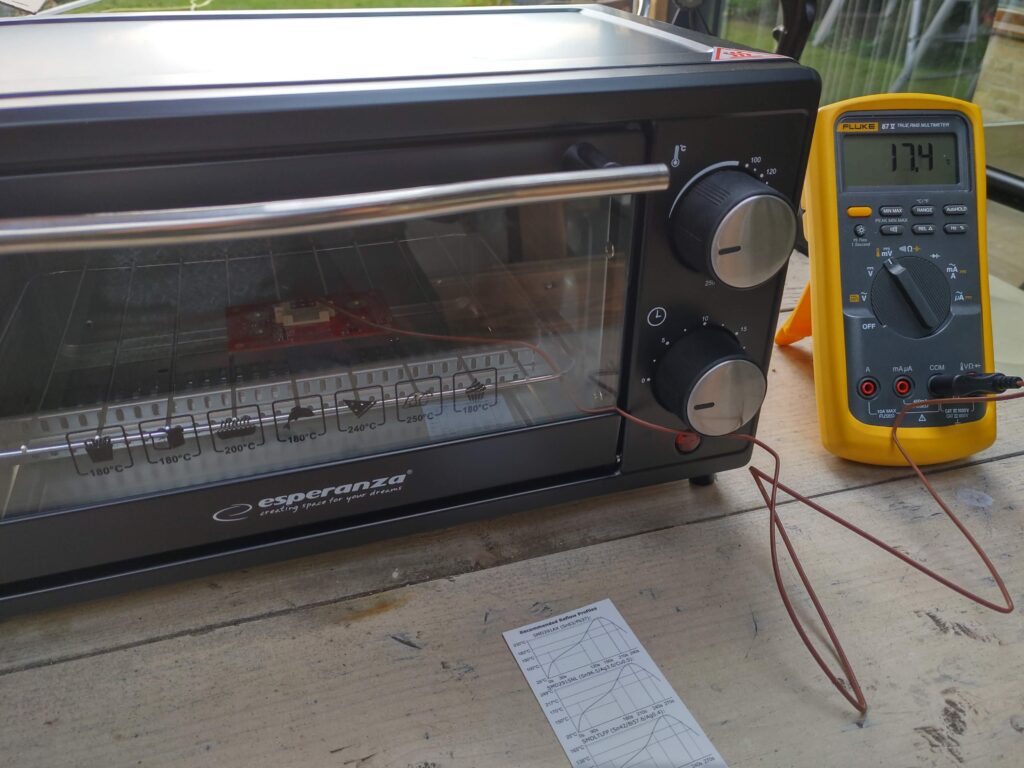
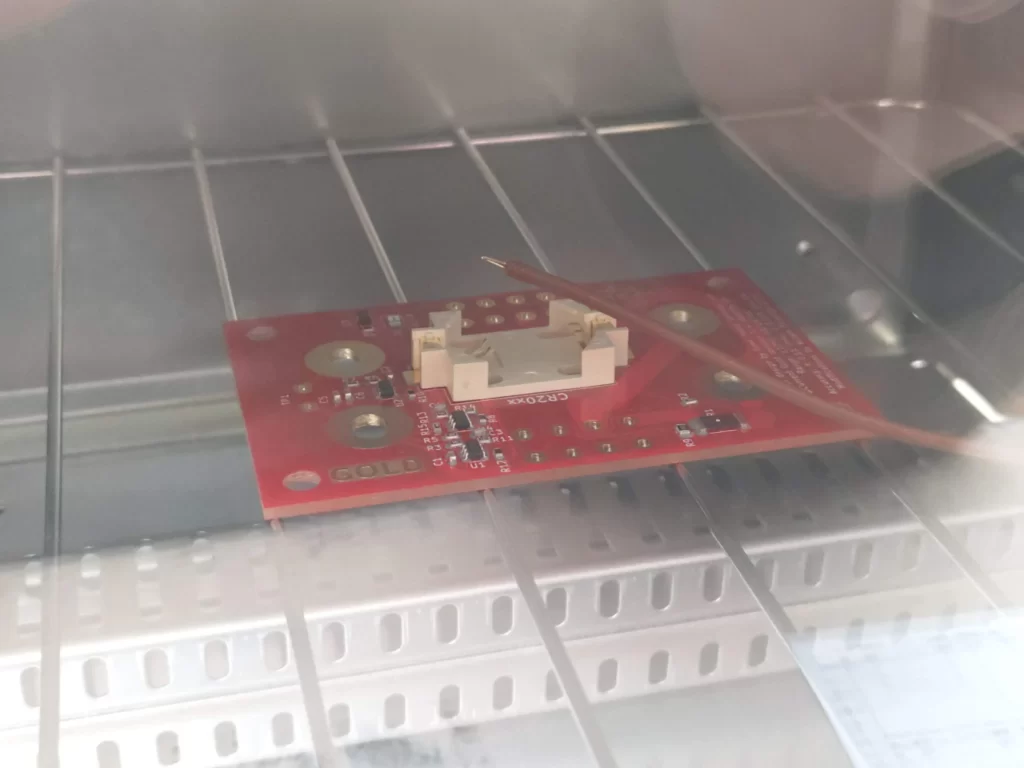
The actual reflow process now begins. The PCB with all SMT components assembled is carefully placed into an oven, together with a K-type temperature probe, because the €30 oven’s thermostat can obviously not be trusted. The probe is just flapping in the breeze slightly above the PCB. In front of me is a piece of paper that shows the recommended reflow temperature over time. I simply follow this trajectory using a stopwatch, the Fluke and constant adjustments of the temperature control on the oven. When peak temperature is reached, I open the oven door to quickly ramp down the temperature. No advanced oven modifications necessary! I’ll probably automate this process in the future since it is quite straightforward to implement and widely documented by other DIY reflowers who have gone before me.


The picture above is the result of my first PCB reflow cycle and I’m super happy with the results. The solder joints look good, there are no bridged pads, and the components seem to have endured the heat quite well. We continue! The reflow process of course only took care of the SMT components, but this device contains some through-hole components, too. In particular, the switches must be soldered and these come with some pretty beefy pins. No worries, these are soldered to the PCB using the regular soldering iron.

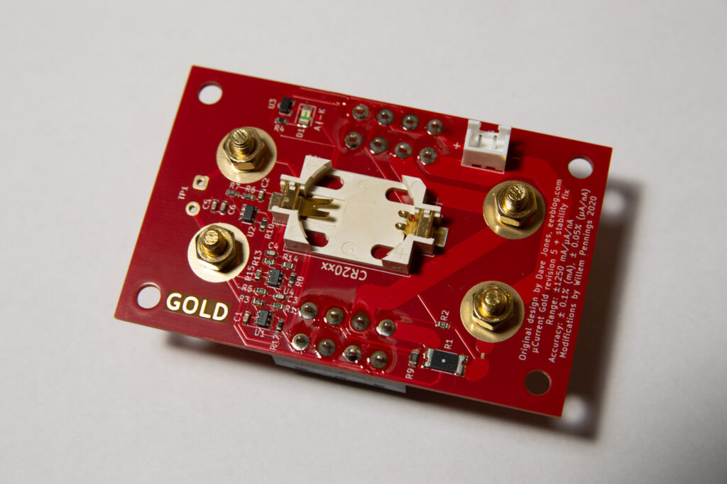
Lastly, the gold-plated binding posts are assembled. These just use a bolt-nut connection. I’m really happy with the quality of the end product.
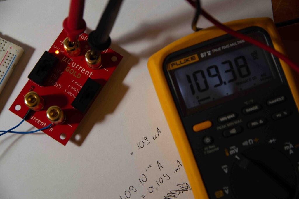
Does it work, though? It turns out that it does. I set up a test current using a fixed-voltage source and a known resistance. The image above shows the test on the uA range, and the multimeter reads the expected value. Perfect! Another great tool in my toolbox, and a new skill picked up along the way.
You can find the Mouser BOM here. I used the original BOM as a guideline. Though not all parts are exactly the same ones as mentioned in the original BOM, almost all parts that I use have identical specifications. The only difference is that R9 has a tolerance of 0.1% instead of 0.05%. As always, feel free to leave a comment if you have any questions about this project.